Application of ALD
- Application of ALD
- Application Window of ALD
Dynamic Random Access Memory
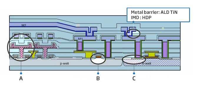
- A
- Cap. dielectric:
- CVD : TaO, BST
- ALD : Al2O3, HfO2, Al2O3 / HfO2
- Electrode :
- ALD : TiN
- CVD : Ru, HSG, PH3/N
- Barrier : ALD TiN
- Capping layer : ALD Al2O3
- B
- Gate electrode : Si – Ge
- Gate dielectric : Al2O3, HfO2
- Nitridation gate
- C
- Contact barrier : ALD TiN
- S/D : SEG with in-situ clean
- STI : HDP
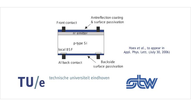
Solar Cell
- ALD Al2O3 for surface passivation of c-Si solar cells
- Bram Hoex, Stephan Heil, Erik Langereis, Richard van de Sanden & Erwin Kessels
Dept. of Applied Physics, Eindhoven University of Technology, The Netherlands - Internet : https://www.tue.nl/en/
Atomic Force Microscopy(AFM)
Objects of almost any size and shape can be coated. Example: AFM tips
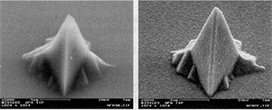
Fig. 1. SEM images of the AFM tips when coated by 30-nm- (left) and 470-nm- (right) thick layers of ALE SnO2M. Utriainen et al. Appl. Phys. A 68 (1999) 339.
Atomic Force Microscopy(AFM)
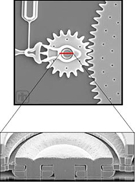
ALD on MEMS Devices
Deposit Ultrathin and Conformal Films on MEMS Devices for:
- Lubrication
- Corrosion Protection
- Higher Hardness
- Tune Mechanical Properties
- Optical Coatings
- Charge Dissipation
- Hydrophobic Surface
* T.M.Mayer, et al., Appl. Phys. Lett. 82 (2003) 2883.
Carbon Nanotube
SAMSUNG-5″ Color display Carbon Nanotube FED
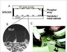
- R.H. Baughman,
- Science 2002, 297, 787
- R.H. Baughman,
- Science 2002, 297, 787.
- C, Dekker,
- Science 2001, 294, 1317.

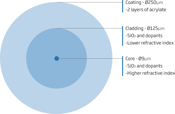
Optical fiber
Standard Single-mode fiber
Barrier Film
Introduction: moisture permeation barriers
Encapsulation of polymeric devices to prevent lifetime degradation by water uptake
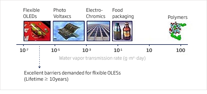
Demands on barrier properties
Gas Sensor & Etc.
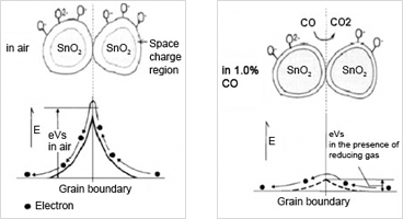
Metal Oxide Semiconductor Gas Sensors
Gas Adsorption on Semiconductor Changes Its Conductivity
Mechanism Involves Changing Carrier Density in space-Charge Region
- Yasuhiro Shimizu and Coworkers :
- Sensors and Actuators B 52 (1998) 38~44